

How to Design a PCB Layout
PCB layout design is a critical phase in the development of any electronic device. It ensures proper alignment and interconnection of electronic components, which is essential for achieving optimal equipment performance. The process involves developing a circuit schematic and using PCB layout software to generate a layout tailored to the product’s specific requirements. Linzhou Electronic Technology (DongGuang) Co., Ltd. offers professional PCB layout services for electronic product developers, supported by its experienced design team.
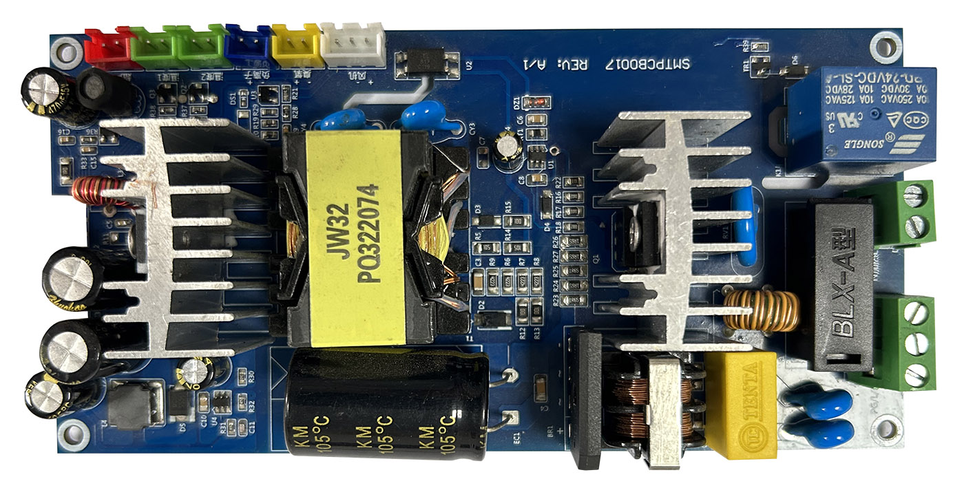
The first step in designing a good PCB layout is to have a clear and complete circuit design. Good circuit design helps reduce the overall time required to produce the final PCB design and minimizes the occurrence of design errors. A circuit design is a schematic diagram showing how electronic components are connected on a circuit board, forming the backbone of a PCB layout. Circuit design software helps simplify this process by allowing designers to drag and drop electronic components into a design and make connections between them. Software utilities such as LabVIEW, Altium Designer, and CircuitMaker can enhance the workflow of the design process.
The second step is PCB layout design. PCB layout design builds on the circuit design and guides the designer through the process of placing each component on the circuit board. PCB layout software such as Eagle PCB, KiCad, and DipTrace allows designers to create a complete and accurate layout, including input and output terminals, vias, power lines, and more. PCB layout software is effective because it allows designers to reduce the size of the board and increase the number of components that can be placed, while reducing the occurrence of design errors.
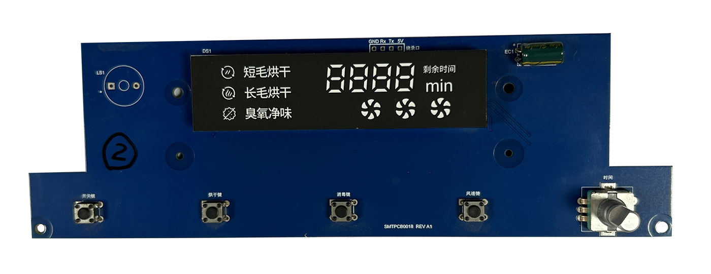
In Linzhou, our professional design team is proficient in a range of electronic product development fields, including software and hardware development, and structural design. When designing PCB layouts, we emphasize functionality, quality, and durability. We are committed to delivering personalized, detail-oriented solutions tailored to meet each customer’s needs. Our PCB layout design process begins with rigorous testing and problem-solving to ensure the project fully satisfies customer requirements. Beyond delivering high-quality products, we strive to build long-term partnerships with our clients.
In summary, the quality of a PCB layout design ultimately determines whether an electronic device will perform optimally. Poorly designed layouts can lead to wiring errors, signal delays, and other issues that degrade device performance. It is essential to develop a clear, complete circuit schematic and leverage professional PCB layout software to create an optimal design. At Dongguan Linzhou Electronic Technology Co., Ltd., our experienced design team helps customers achieve this goal through comprehensive PCB layout services. Contact us today to learn more.
Post time: Jun-03-2019