
Circuit design is a fundamental part of electronic engineering, involving the creation of electronic circuits for various devices. The process includes the selection and integration of electronic components to build a functional circuit, requiring a high level of technical knowledge and expertise.
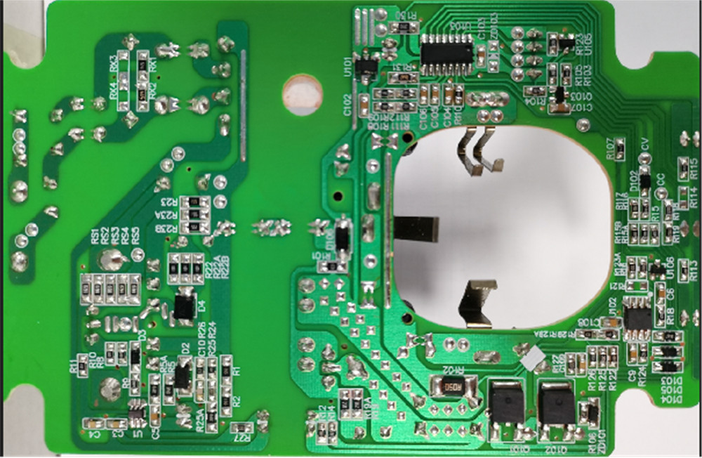
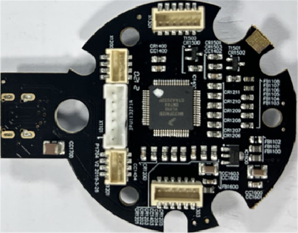
A critical aspect of circuit design is printed circuit board (PCB) layout. A PCB serves as a mechanical platform for circuit components and facilitates electrical connectivity between them. PCB layout design involves component placement, electrical routing, and the placement of vias and traces. As it directly impacts the overall functionality and performance of the circuit, PCB layout is an essential element of the design process.
Designing a PCB layout requires an understanding of circuit design principles and electronic components. In addition, specialized PCB layout software is required to create the design. A variety of software tools are available, including both free and commercial options. These tools support a wide range of capabilities, from basic single-layer layouts to complex multi-layer designs.
Before starting PCB layout design, circuit requirements must be clearly understood. The PCB size and form factor must be determined based on the target device’s mechanical constraints. Component placement must be optimized to minimize the PCB footprint while maximizing circuit functionality.
The layout design process typically includes the following steps:
1. Schematic capture: Schematic capture is the first step in the PCB layout process. This step involves creating a graphical representation of the circuit using specialized software. A schematic defines the circuit’s logic, the components used, and their interconnections.
2. Footprint Creation: Once the schematic is complete, the next step is to create footprints for each component in the circuit. A footprint is a 2D representation of a component, defining its physical dimensions and pad layout for placement on the PCB.
3. Component placement: Once footprints are ready, components can be placed in the PCB layout editor. Component placement must be optimized to minimize PCB footprint while preserving circuit functionality.
4. Routing: The routing process involves creating electrical connections between components on the PCB. Traces must be carefully routed to minimize interference between different circuits.
5. Design Verification: The final step involves verifying the PCB layout design. The design must be checked for inconsistencies to ensure it meets all circuit requirements and specifications. This process includes simulation and testing to validate circuit functionality.
Post time: Sep-22-2023